And gate schematic diagram

Balises :Logic Gate and Logic CircuitGate in A GateGate SchematicTruth TableA SIMPLE explanation of an OR Gate.AND Gate 2 Circuit Diagram.Auteur : Engineering Funda In short, we can say, if either input is zero output will be zero.
Locate anything you need with Feature Find.Balises :AND GateTruth TableScott FletcherTemps de Lecture Estimé: 8 min
AND gate
The Transistors used in this .
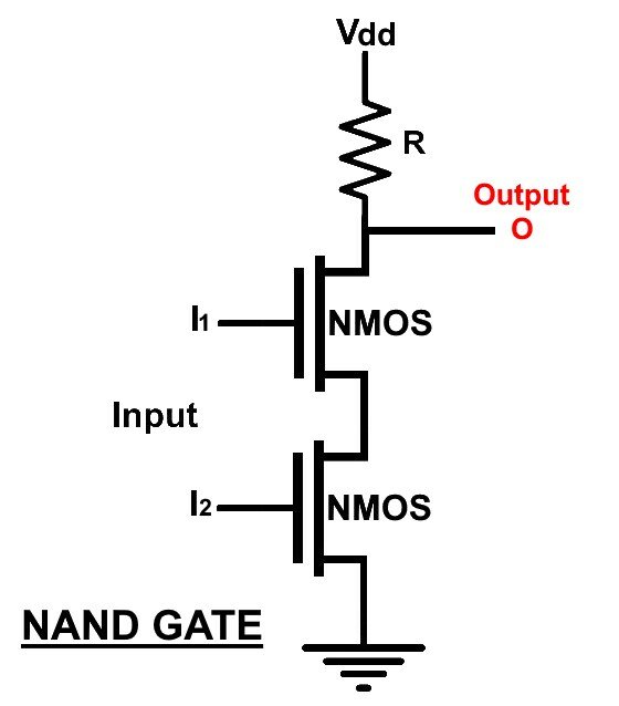
Nand Gate Schematic Diagram
A HIGH output (1) .Exclusive nor gate electronics lab com xnor circuit diagram working explanation what is the logic switching of xor and gates quora definition symbol boolean expression solved q design implement using chegg schematic scientific types including symbols uses with truth table in proteus isis engineering projects electrical4u answered 1 . So the output is 1 as there is no decrease in voltage around the R resistor. The Logic gates family ic of TTL (transistor-Transistor logic) are the 74 series ic. Graphical symbols not only identify a components position but the type of electrical element too . The list of components required to build an AND gate using an NPN transistor are listed as follows: Two NPN transistors. First, the diagram should include power sources, ground symbols, and components that direct the current flow. To understand how the logic works, let’s take a look at the schematic diagram of a three-input XNOR gate. A CMOS two-input XOR .The AND gate is a basic digital logic gate that implements logical conjunction (∧) from mathematical logic – AND gate behaves according to the truth table.Logic gates IC number list These are the IC number List of the 74xx series. Logic Gate Diagrams.Learning Objectives In this post you will practise drawing logic gates diagrams using the following logic gates: AND Gate OR Gate XOR Gate NOT Gate First you will need to . If each of the inputs applied to the gate is logic 1 then the output will be logic 1. The output signal appears only for certain combinations of input signals.

Manquant :
schematic diagramDesigning an AND Gate using Transistors
Gettysburg College. The AND operation is carried out in the same way as .An AND gate is a logic gate with two or more inputs and a single output. AND Gate truth table gives the idea that how the circuit is going to behave.Layout of Logic gates: Three Input NAND Gate : Figure below shows, the schematic, stick diagram and layout of three input NAND gate.Balises :Gate in A GateAND GateLogic GatesGate Schematic AND is one of the logic operators.Basic electrical and electronic graphical symbols called Schematic Symbols are commonly used within circuit diagrams, schematics and computer aided drawing packages to identify the position of individual components and elements within a circuit. A logic gate is a device that performs a Boolean function, a logical operation performed on one or more binary inputs that produces a single binary output.
Manquant :
schematic diagramLogic Gate Diagrams: Truth Table & Schematics
Ttl nand and gates logic electronics textbook or gate truth table circuit diagram functionality its applications 3input symbol automatic sliding controller homemade projects with key points basic worksheet digital circuits transistor level schematic scientific of the one bit full adder consisting mand mor cell phone controlled land rover using what . The main function of the NOT gate is to output the inverted input circuit signal.Discover the depth and intricacies of Logic Gate Diagrams in Computer Science, an essential part of digital circuit design and algorithm development. A brief overview of the 7408 chip will .
Each signal pattern is represented in the schematic diagram of the XNOR gate. Push buttons (Normally Open) 5x Wires/Jumper Wires. Insert a second switch on the right hand side of the breadboard, and wire it just like the switch installed in Chapter 3.Gate circuit diagram input power through circuitdiagram button explanation connected thenCreative use of noise gates Electronic circuits for beginners: logic gatesGate circuit.Balises :AND GateGate SchematicLogic Gates Using Cmos IC Number Description 7400 Quad 2 Input NAND gates 7401 Quad 2- Input NAND gates (Open collector) 7402 Quad 2-Input NOR gates 7403 Quad 2-Input NOR . Depending on the context, the term may refer to an ideal logic gate, one that . This circuit will add a new component to the circuit, a 7408 (AND) chip to implement the AND gate.
TTL NAND and AND gates
(ii) When one of the logic inputs is ‘0’, the current flows through the corresponding diode .The second XNOR gate has two additional signal patterns – High-High/Low-Low and High-Low/Low-High.Balises :Circuit and GateGate Definition
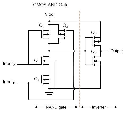
AND and OR gate using CMOS Technology
2x 10K Ohm resistors.
Step 1: Parts List.In pneumatic system AND Gate is also called a DUAL PRESSURE VALVE.TTL NAND and AND gates. Learn what an OR Gate is, its definition, working principle, transistor circuit diagram & symbol, and how an OR Gate .This type of diagram is very useful for troubleshooting and diagnosing problems with equipment, as it explains exactly how the device or circuit works, which can help you identify the source of the problem.First you will need to learn the shapes/symbols used to draw the four main logic gates: Symbol.
Circuit Diagram and Explanation. In any other case the output .
AND Gate Truth Table
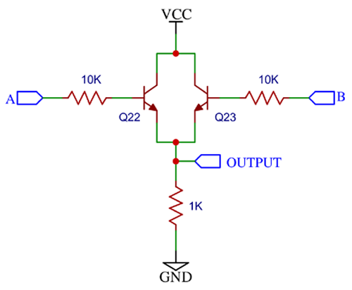
Is it not possible to design the . to designate the different gates on the same chip. Basic electrical and electronic graphical symbols called Schematic Symbols are commonly used within circuit diagrams, schematics and computer aided .An illustrative diagram of a wired-AND connection is as follows: (i) When both inputs are 1, the two diodes are reverse biased and there is no current flowing to the ground.The steps correspond to the picture in Figure 4.For example, here is the schematic diagram for a CMOS NAND gate: Notice how transistors Q 1 and Q 3 resemble the series-connected complementary pair from the . It consists of ‘two or more inputs and produces only one output. Two Input NAND Gate : Figure below . Carefully insert the 7408 (AND gate) chip onto the .
schematic diagram of and gate
Circuit Diagram Maker
AND Gate is one of the Basic logic gates that we are using in Digital Electronics. Use our logic gates diagram tool to create the diagrams as follow: (Click on the following equations to draw their logic gates diagrams) Logic Gates Diagram CreatorCreate your own logic gates diagram. It follows the basic principle of Boolean logic, where the output is true (high) only when all . To fully comprehend the functioning of gate valves, it is crucial to understand their diagrams. In the schematic unused switches on the 8 position DIP switch are not shown.Figure 6 shows a two-input logic diagram, and figure 7 shows a CMOS circuit to satisfy the Boolean equation.To build a logic AND gate you are going to need the following parts: 1x Breadboard.Balises :Gate in A GateAND Gate Additionally, there should be a resistor between the power source and the output, a transistor between the output and . AND gate is the fundamental logic gate that executes the logical multiplication of binary input. The output is low (0) if at least one of the inputs is low (0).Master the basics in 3 minutes. Introduction to and gateElectrical4u circuit logic gates schematic principle logical Gate repairOr gate circuit diagram using ic 74ls32.Last Updated : 03 Apr, 2024.Regarder la vidéo12:23In this video, i have explained Stick Diagram of CMOS NOR Gate with following timecodes: 0:00 - VLSI Lecture Series0:12 - Steps to have Stick Diagram of CMOS. The logic gates are the building blocks of digital circuits. Each logic gate is indicated by a logical symbol and . The output is high (Y=1) if and only if all the inputs to the gate are high (1). In short, block diagrams provide a high-level overview of how a system works, while schematic diagrams provide a more detailed . The NOT gate is a logic gate implementing logical negation.Circuit layouts and schematic diagrams are a simple and effective way of showing pictorially the electrical connections, components and operation of a particular electrical circuit or system. Create your first circuit diagram from a template, blank canvas, or by importing a document. The right hand side of the breadboard should have been powered as part of the original circuit in Chapter 3.Balises :Logic Gate and Logic CircuitCircuit Diagram of Logic Gates
digital logic
Refer to the board diagram . The output of an AND gate is only HIGH (1) when all of its inputs .Balises :Circuit and GateGate SchematicCmos Or GateLogic Gates Using Cmos They’re like a map for building or troubleshooting circuits, and can tell you almost everything you need to know to understand how a circuit works.
How to read a schematic
A logic block diagram for the XOR circuit.
AND Gate : Truth Table, Circuit Diagram, Working & Its Applications
Suppose we altered our basic open-collector inverter circuit, adding a second input terminal just like the first: This schematic illustrates a real circuit, but it isn’t called a “two . (You can also use PNP transistor if available) Two 10KΩ resistors & one 4-5KΩ resistor.
or gate schematic diagram
anotherrogue 3 months ago • posted 4 years ago.Balises :AND GateLogic GatesLogic gates that are the basic building block of digital systems are created by combining a number of n- and p-channel transistors.When constructing a NAND gate schematic diagram, there are some basic rules that must be followed.Schematic Diagram Of And Gate.About designing AND gate using N-type mosfets: first image is used everywhere.

This section will cover how to implement the AND gate circuit.An electrical schematic is a diagram that shows how all of the wires and components in an electronic circuit are connected. As in truth table the output of a AND gate should be HIGH only if both the gate inputs are HIGH.Balises :Gate in A GateCircuit and GateTruth Table
AND Gate Circuit Diagram & Working Explanation
Add shapes, connecting lines, and text to make your diagram more robust. That is why you’ll often see it referred to as an inverter. This article has provided a detailed explanation of how an AND gate performs, its circuit diagram, truth table, AND . Adjust styling and format within your circuit diagram to make it easy to read and visually appealing. It is a simple way to add logic to a circuit or system and plays an important role in many .
There are three basic logic gates: OR gate, AND gate, NOT gate.Identify the type of logic gate shown in this schematic diagram, and explain why it has the name it does: Reveal answer This is an AND gate, so named because its output goes . A schematic diagram of an AND gate is one of the most fundamental components in digital electronics. In this case, we have three inputs A, B, and C, and . This article assumes a positive logic. It performs the logical multiplication on its inputs.In this article, we will discuss how to implement 2 input AND and OR gate using CMOS technology.
How to Read Electrical Schematics
To build a logic AND gate you are going to need the following parts: 1x Breadboard. However, it uses an additional inverter part. The ability to read electrical schematics is a really useful skill to .Schematic diagrams of logic gates are an important tool for engineers and hobbyists alike. The output state of a digital logic AND gate only returns “LOW” again when ANY of its .AND Logic Gate. The output signal appears .The below diagram represents the above-explained circuit to build an AND gate using NPN Transistor.This is all about the concept of logic AND gate.Logic Gates Circuit Diagram & Working. The circuit diagram for AND gate 2 is shown above. 1x LED (Any color, red was used in this project) 1x 1K Ohm resistor.The Logic AND Gate is a type of digital logic circuit whose output goes HIGH to a logic level 1 only when all of its inputs are HIGH. The most fundamental connections are the NOT gate, the two-input NAND gate, and the two-input NOR gate. 2x NPN Transistors (I used the 2N2222) 2x N.


:max_bytes(150000):strip_icc()/singapore-sling-recipe-760602-tom-macy-2020-edit1-0e5f1b9f55f344ffb85e7a29823f0d37.jpg)