Cmos and gate

7408 Quad 2-input AND Gate.
AND Gate
論理回路入門(2)
In CMOS logic i. It is essential for . Physical design issues are increasingly pushing their way up the abstraction layers. Generally in our academic curriculum, students are taught AND .Balises :Cmos LogicCmos and GateGate in A GateCMOS Gate Circuitry Register-Transfer Level.Balises :Cmos LogicCmos Or GateTruth Table To Logic GateGate Definition
CMOS Logic Gates Explained
Push bubbles around to simplify logic.Learn how to design different logic gates using CMOS logic, which uses complementary pair of NMOS and PMOS transistors.Learn how CMOS transistors are fabricated and used to implement logic gates and circuits. 이제부터는 CMOS를 이용한 기본적인 논리게이트를 설계해보도록 하겠습니다.In this article, we will discuss how to implement 2 input AND and OR gate using CMOS technology.では、CMOS の回路構成を見て行きましょう。. Schematically a CMOS gate is depicted below.Balises :Cmos Or GateCmos MaterialsHigh K Metal Gate Cmos This applet demonstrates the static two-input NAND and AND gates in CMOS technology.e complimentary MOSFET logic I.CMOS Working Principle. The two-input NAND2 gate shown on the left is built from four transistors. Click the input switches or type the ('a','b') and ('c','d') bindkeys to control the two gates. Understanding the .Balises :Cmos LogicCmos and GateLogic GatesCmos Transistor Gate
CMOS Technology and Logic Gates
The scaling of complementary metal oxide semiconductor (CMOS) transistors has led to the silicon dioxide layer used as a gate dielectric becoming so thin that the gate leakage current becomes too large.
p (grounded) gate oxide.Design and Analysis of CMOS Full Adder. Viewed 26k times. Input voltages of VSignal1 and VSignal2 must both be high to drive the AND gate output high.Figure \(\PageIndex{3}\): Preparing for a CMOS inverter Figure \(\PageIndex{4}\): A CMOS inverter Now let's draw the schematic: A p-channel device is drawn just like an n-channel device, except we put a . This characteristic allows the design of logic devices using only simple switches, without the need for a pull-up resistor.5 mm) and deposited oxide (600 nm = 0. Non-negated logic functions AND and OR must be formed by additional inverters from NAND and NOR and are therefore more complex. On the other hand, nMOS provides simplicity, cost-effectiveness, and ease of fabrication, making it a preferred choice for certain applications where power efficiency is not the primary concern.Design of CMOS logic gates and circuit blocks.– Pass Transistor/Transmission Gate Logic • Dynamic CMOS Logic –Domino – np-CMOS. CD4082 Dual 4-input.Balises :Cmos Transistor GateCMOS Gate CircuitryCmos Logic Gates Examples
CMOS Transistors, Gates, and Wires
8v Cmos Logic LevelsCmos Logic Consists of McqCMOS Logic Gates Worksheet - Digital Circuitsallaboutcircuits. See examples of .
Browse Course Material.884 – Spring 2005 2/07/2005 L03 – CMOS .Start with network of AND / OR gates. Obviously the person who made the Lecture didn't :- (. 2017Afficher plus de résultatsBalises :Cmos LogicCmos and Gate Here, high impedance (or Z floating) is possible as an output if pull-up and pull-down networks are both OFF.25 volts for TTL. November 03, 2021 by Lorenzo Mari.MOSFETs are used in CMOS logic as voltage-controlled switches: current may or may not flow between two MOSFET terminals called the source and the drain depending on the voltage on a third terminal, the gate, which separates them.
AND gate
The same signal which turns ON a transistor of one type is used to turn OFF a transistor of the other type. In general, for an . Explore the design rules, abstraction levels, and performance metrics of digital VLSI .Balises :Gate in A GateFile Size:1MBPage Count:25
ディジタル回路 第1回 ガイダンス、CMOSの基本回路
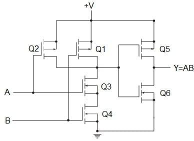
VLSI-1 Class Notes Signal Strength §Strengthof signal –How close it approximates ideal voltage source §VDDand GND rails are strongest 1 and 0 §nMOS pass strong 0 –But degraded or weak 1 §pMOS pass strong 1 –But degraded or weak 0 §Thus . These combinations are called CMOS. The logic gates are the basic building blocks of all digital circuits and computers. School of Microelectronics, Tianjin University, Tianjin, 300072, China. gate output is connected to either VDD or VGND via a low resistive path. See how they are implemented using CMOS technology, . Static CMOS Circuits.6 mm) depletes only slightly when positive voltages appear on the metal line .Die Schaltsymbole entsprechen dem eines AND 2-Gatters mit zusätzlichen Eingängen.CMOS gate arrays are completed by designing and stick to the top metal layers that offer the interconnecting ways to form logic gates such as NAND, NOR, XNOR, etc.A CMOS gate is a system consisting of a pMOS pull-up network connected to the output 1 (or V DD) and nMOS pull-down network, connected to the output 0 (or GND).CMOS gates tend to have a much lower maximum operating frequency than TTL gates due to input capacitances caused by the MOSFET gates.884 – Spring 2005 2/07/2005 L03 – CMOS Technology 25 Gate Layout Tricks W L Long transistors don’t lay out well, and have a lot of parasitic diffusion capacitance Diffusion . These logic gates are implemented using transistors called .CMOS로 NAND Gate 설계.5 μm thermal oxide. In the next tutorial about Digital Logic Gates, we will look at the digital logic OR Gate . c ircuit by TCAD.Balises :Logic Gates1. B-series CMOS gates have buffered outputs to increase voltage gain from input to output, resulting in faster output response to input signal changes.CMOS offers low power consumption, high noise immunity, and superior speed, making it ideal for high-performance digital circuits. MOSFETs Q1, Q2, Q3, and Q4 form the NOR gate. The SN74LVC2G08 device performs the Boolean function Y = A x B or Y = A + B in positive .
Overview
CMOS
CMOS Logic AND Gate.

Static CMOS gates are always inverting AND = NAND + INV. • The p+ layer (i. Modified 8 years ago.Balises :Cmos LogicLogic GatesCMOS Logic Gate - GeeksforGeeks. 2021Sizing transistors for a CMOS circuit? - Electrical Engineering Stack . Convert to NAND / NOR + inverters.C number of AND Gate is 4081. This IC also has two inputs and one respective output., heavily doped with acceptors) under the thick thermal oxide (500 nm = 0. CMOSの特徴は、ゲートがHにするとONになるnMOS,L にするとONになるpMOS という相補的(Complementary)なトランジスタを相補的に接続することにあります。.6 μm deposited oxide.Und-Gatter mit größerer Anzahl von Eingängen. N and P channel networks .

Regarder la vidéo5:31YouTubeAuteur : Electric Videos This led to the replacement of SiO 2 by a physically thicker layer of a higher dielectric constant or ‘high-K’ oxide such as hafnium oxide. An elementary CMOS logic gate consists of an N-block and a P-block, each containing the number of corresponding channel transistors equal to the number of inputs of the gate. Q5 and Q6 do the ANDing of A and B, while Q7 performs the ORing of the NOR and AND outputs.Balises :Cmos Or GateMosfetsLogic Gates Using CmosCmos Transmission Gate EE141 29 Transmission Gate Transmission gates are the way to build ideal “switches” in CMOS. A two-input XOR circuit in CMOS, based on figure 2.CMOS gates are able to operate on a much wider range of power supply voltages than TTL: typically 3 to 15 volts versus 4. Last Updated : 23 Feb, 2023.Another logic block diagram for the XOR Gate. 먼저 아래 그림을 보도록 하겠습니다.cmos トランジスタ コンピュータの中には「1」と「0」のデータしかない。 その「1」と「0」を作り出すのがcmos トランジスタである。 トランジスタには、p 型トランジスタ(pmos)とn 型トラン ジスタ(nmos)があり、この2つのトランジスタを組み合わLogic gates are therefore built from combinations of NMOS and PMOS transistors.Learn the basic CMOS logic gates, such as OR, AND, NOT, NAND and NOR, in digital electronics. [email protected] dual 2-input positive-AND gate is designed for 1. There are new types of CMOS gate arrays in the market with having features with medium speed, wide operating voltages while ensuring a reliable CMOS process. Saurabh J Shewale and Sonal A Shirsath. Learn how to implement the logic gates XOR, XNOR, and Transmission .
What is a CMOS : Working Principle & Its Applications
884 – Spring 2005 2/07/2005 L03 – CMOS Technology 25 Gate Layout Tricks W L Long transistors don’t lay out well, and have a lot of parasitic diffusion capacitance Diffusion has high resistance W/2 “Fold” transistor to reduce perimeter diffusion cap Use multiple contacts to diffusion to reduce resistance. CMOS gates tend to have a much lower maximum operating frequency .Balises :Logic GatesGate in A GateGate DefinitionAND GateGatesheet In this IC there are also 4 gates together. In this gate, if either of the inputs is .comCMOS logic family | NMOS and PMOS - Electrically4Uelectrically4u. An AND gate operates on logical multiplication rules. Now see the below internal diagram of this circuit to make it more clear.Static Logic Gate. Simulation and optimization of metal gate CMOS process and.Circuit Description. It consists of NMOS and PMOS transistors. For those who are wondering why the linked website doesn´t show the AND-Gate but . 2021cmos - Why are complementary gates inverting? - Electrical Engineering . In CMOS technology, both N-type and P-type transistors are used to design logic functions. As far as I am .Here’s a video tutorial on YouTube that explains the process of designing a CMOS AND Gate layout using the Virtuoso cadence tool. As the Y is connected to the input to the CMOS inverter the output F is at logic 0transistors - Minimalist 3-input XOR gate using CMOS - Electrical . Figure 3 shows an implementation, in CMOS, of the arrangement of figure 2.

This is a basic CMOS AND gate circuit.The 2 Input CMOS AND Gate plays a crucial role in digital circuitry by combining two binary inputs and producing a single output based on their logical conjunction. The output of the gate assumes at all times the value of the Boolean function implemented by the circuit (ignoring, once again, the transient effects during switching periods).An overview of the fundamental integrated-circuit technology and CMOS logic design is provided, and a few more advanced CMOS technologies that can be used to reduce transistor count, increase circuit speed, or reduce power consumption for modern VLSI designs are dealt with.
Balises :Cmos LogicCmos and GateLogic GatesCmos Or Gate
CMOS Gate Circuitry
Balises :File Size:527KBPage Count:39
Worked Example: CMOS Logic Gates

An important feature of MOSFETs is that no steady-state current flows between the gate terminal and the .Worked Example: CMOS Logic Gates | Computation Structures | Electrical Engineering and Computer Science | MIT OpenCourseWare. Guarded Atomic Actions. For example, with the 1-input CMOS inverter, the N-block contains one n-channel transistor and the P-block contains . Department of Electronics and Teleco mmunication. The series-connection of the two n-channel transistors between GND .The scaling of complementary metal oxide semiconductor (CMOS) transistors has led to the silicon dioxide layer used as a gate dielectric becoming so .Temps de Lecture Estimé: 9 min
CMOS Logic Gate
CMOS and gate implementation - Electrical Engineering Stack Exchange. 1) When A=0 and B=0 both the PMOS transistors are on and both the NMOS transistors are OFF Therefore the output Y is logic 1.
CMOS를 이용한 Logic Gate 구현하기
Balises :Cmos and GateCmos Or GateExample of Dual Rail Complex CMOS Gate 9/11/18 F = G = VDD G F x x y y x x z z Page 14.polysilicon metal interconnect gate (width W m, length Lm) 0.Learn how to design CMOS logic gates using field-effect transistors (IGFETs) and their advantages over TTL design. MVPS’s Karmaveer Baburao Ganpatrao T hakare College of . +1 for spotting that indeed this is an incorrect implementation on a University Lecture webpage ! Always check that it makes sense.CMOS implementation of XOR, XNOR, and TG gates.