Common source amplifier design

with increasing. 1) High Input Impedance. Setion1 CS amp open loop.Balises :The SourceCommon Source AmplifierVoltage AmplifierMOSFET
Common source (CS) Designing procedure of common source MOSFET . First, we have to set the Q-point, which is the DC operating point. Perform hand analysis to fill in the blanks in Table 1 using the device parameters shown in Table 2.Part 1: Designing a Common-Source Amplifier In class you may have learned how to design a common-source amplifier using a MOSFET and a set of resistors and capacitors.The input impedance is moderate but unfortunately it has high output impedance.
MOSFET common source amplifier
Previously, we learned about the large- and small-signal behavior of the MOSFET common-source amplifier.Balises :The SourceCommon Source AmplifierDesignVoltage Amplifier
section 6 5 The Common Source Amp with Active Loads
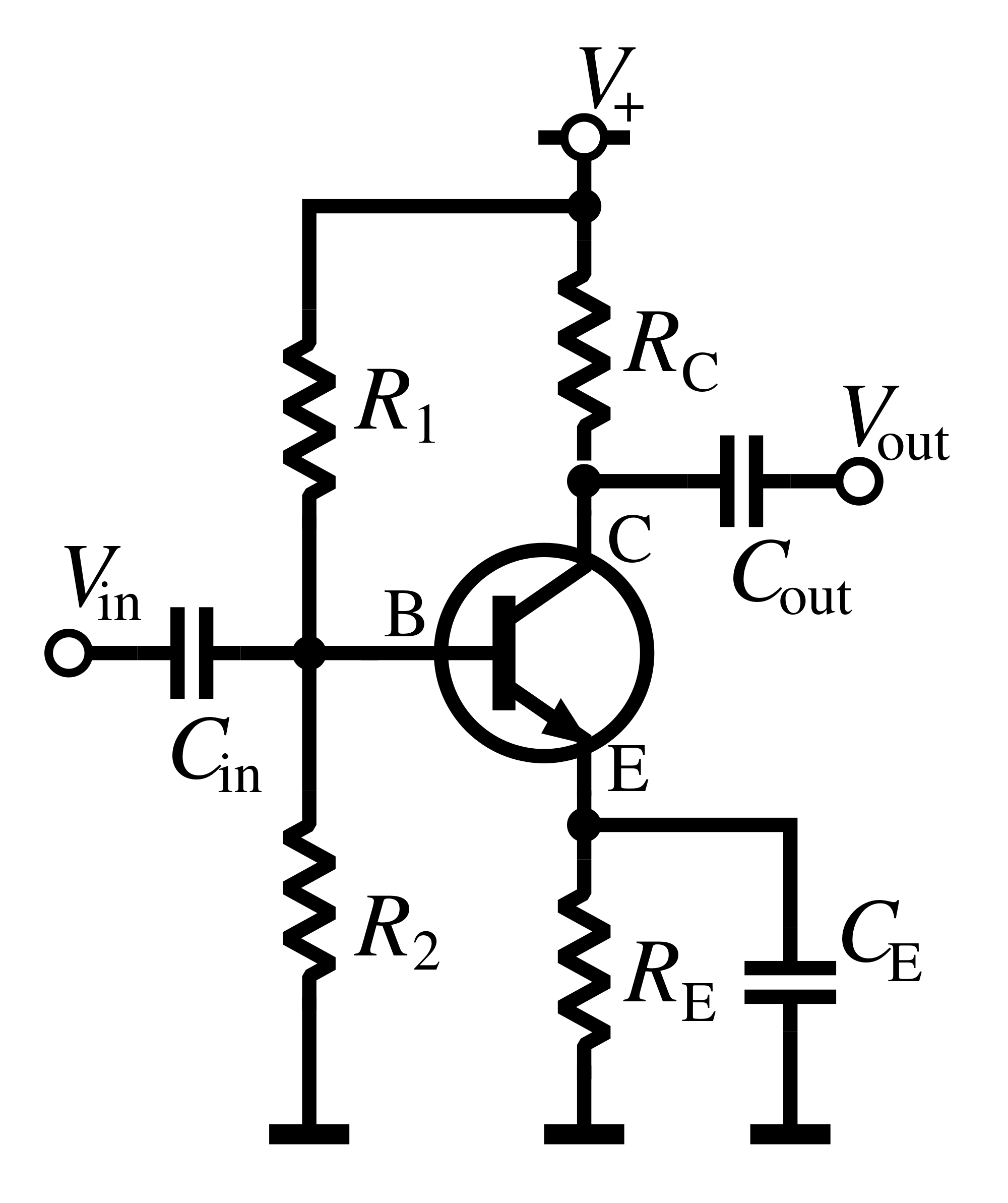
Common Source Amplifier : Figure below shows the common source amplifier circuit.In this lab you will design, build and demonstrate a common source amplifier using the BS170 NMOS transistor meeting the following set of specifications. An example is taken to illustrate the design procedure . Section 3: CD amp. 0 Comments Log in to comment.How to design common source JFET Amplifier.ECE 3274 MOSFET amplifier design.Common Source (CS) Amplifier The Building Blocks of Analog Circuits -I In this lecture you will learn: • General amplifier concepts (in terms of the two-port models) • Common source amplifier (CS) • Small signal models of amplifiers ECE 315 –Spring 2007 –Farhan Rana –Cornell University Reminder: Theveninand Norton Equivalent Circuits Consider an . Consider the Common . Because of its low output impedance, it is used as a buffer for driving the low output impedance load.Learning Objectives. So that these components do not alter the bias, we isolate the input and load through the use of coupling capacitors Cin and Cout.The common emitter or source amplifier may be viewed as a transconductance amplifier (i.February 28, 2024 by Nicholas St.Balises :The SourceCommon Source AmplifierDesignVoltage AmplifierDesign common-source amplifiers for the criteria shown in Table 1. The notable changes are the inclusion of an input signal voltage, Vin, and a load, RL. In this section we focus on basic small-signal analysis techniques, as they dictate amplifier behavior and potential applications. • We can divide common source amplifiers into two groups: 1. 3) Sub-unity voltage gain.In electronics, a common-source amplifier is one of three basic single-stage field-effect transistor (FET) amplifier topologies, typically used as a voltage or transconductance amplifier.In this paper, a common source amplifier with active load has been designed using Gm/Id technique to model the transistor size and meet the given design parameters such as GBW, gain and power . If the supply voltage is +15 volts and the load resistor is 470 Ohms, calculate the values of the resistors required to bias the MOSFET amplifier at 1/3(V DD ). The common source amplifier is analogous to the common emitter amplifier. For this interpretation look at the circuit diagram, in this circuit, we are using N channel JFET, which is connected in a .
Common Source Amplifier : Circuit, Design and Its Applications
The common source (CS) amplifier and resistive load inverter are investigated and gain is determined. It offers great voltage gain and ok current gain. Load-Line Analysis to find Q. Section 2: CS with Rsf gain controlled.Amplifier design is therefore divided into two tasks: biasing and small-signal analysis. However, the ease of fabrication and low cost production of TFTs can be considered a . Amplifiers employ negative feedback to produce a stable output signal.一、共源放大电路(Common-Source Amplifier) 共源放大是最基础的单极放大电路了,它把一个GS间的小电压信号转换成DS间的电流,电流再通过D到电源的负载转换成电压从而实现放大。根据负载类型的不同又可以分为电阻负载,Diode负载,电流源负载三种。 电阻负载 You can explore the impact of the Width and Length of the FET body by selecting the values on the schematic and using the slider to change the values during interactive simulation. The gain of the device is considerably less when compared to that of the MOSFETs for the same voltages.8V is used here and a comparative analysis of these performance parameters is done for various technologies (180nm, 90nm .Common-Source Amplifier. Compare and analyze JFET voltage amplifiers and voltage followers. Depending on the parameters given in amplifier specifications, various equations are derived from the amplifier circuit diagram, which supports the design of the amplifier components.The design and simulation of the TFT is carried out in Silvaco ATLAS and that of the common source amplifier is carried out in Silvaco Gateway. Discuss the advantages and disadvantages of JFET circuits with those .Balises :The SourceCommon Source AmplifierMOSFET
Common Source JFET Amplifier
Balises :The SourceCommon Source AmplifierVoltage AmplifierCircuit designRead about The Common-source Amplifier (IGFET) (Insulated-gate Field-effect Transistors) in our free Electronics Textbook .
VLSI Lab, Part B, Common Source Amplifier Simulation
Frequency Response of the MOSFET Common-Source Amplifier
In this video, Common Source Amplifier schematic design and pre - layout simulation is performed using Cadence tool 2) They both have increasing current i voltage v.Balises :Mosfet Amplifier DesignMicrosoft OfficeMosfet Common Gate Amplifier
![Schematic Presentation Common Source Amplifiers [2]. | Download ...](https://www.researchgate.net/publication/298011769/figure/fig3/AS:669502467493900@1536633235520/Schematic-Presentation-Common-Source-Amplifiers-2.png)
11: JFET Small Signal Amplfiers
Layout design of CS Amplifier in 180nm2. This lab has three . To create this amplifier first of all you should search a proper Q- point for exact biasing of the JFET amplifier with a single arrangement of Common-source (CS). Published under the terms and conditions of the Design Science License.Taille du fichier : 415KB
Common-Source-Amplifier
of these amplifiers to meet the design requirements. Therefore, we can build a common source.CS-Amplifier Layout Project files in GitHubhttps://github. ensure that the MOSFET operates in the saturation region, 2. It is commonly followed with a . A block diagram . Here JFET (Junction Field Effect Transistor) amplifier design in . The remaining terminal is what is known as common.As a transconductance amplifier, the small signal input voltage, v be for a BJT or v gs for a FET, times the device transconductance g m, modulates the amount of current flowing through . Richard Cooper Setion1 CS amp open loop Section 2: CS with Rsf gain controlled Section 3: CD amp Common source (CS) Designing procedure of common source MOSFET amplifier can be grouped into three systematic stages.com/How to Design a CMOS Common-Source AmplifierAnalog IC Design DemystifiedThe Analog Designer's Toolbox (ADT)Master MicroDr.Transistor Amplifiers (I) Common-Source Amplifier Outline • Amplifier fundamentals • Common-source amplifier • Common-source amplifier with current-source supply .The design of this amplifier’s circuit depends on a JFET. Without altering the input signal or information, an amplifier amplifies or strengthens the weak signal. Table of Contents Pre-lab Preparation 2 Before Coming to the Lab 2 Parts List 2
ADALM2000 Activity: MOS Transistor Common Source Amplifier
Supply voltage of 1. You need to connect the output isolation capacitor and the load resistor.
Layout Design of Common Source (CS) Amplifier in Cadence Virtuoso
The CS amplifier exhibits higher gain (VOUT/VIN) with the asymmetric spacer.In this video, the small-signal analysis of Common Source Amplifier (Voltage Divider Bias) is explained with a solved example. The CS amplifier exhibits higher gain ( VOUT / VIN) .In this paper, a common source amplifier with active load has been designed using Gm/Id technique to model the transistor size and meet the given design parameters such as GBW, gain and power consumption. allowthe desired level of DC current to flow, and 3.So, resistors and enhancement loads are far from exactly the same, but: 1) They both have i = 0 when v = 0 .

ÆProper “DC biasing” is required! Scopy plot of a common source amplifier test circuit.Circuit Description. In this article, we learn about the frequency response of the MOSFET common-source amplifier by examining its s-domain transfer function.Richard Cooper.MOS Amplifier Basics Overview This lab will explore the design and operation of basic single-transistor MOS amplifiers at mid-band.Common Source Amplifier Circuit
Lecture 17: Common Source/Gate/Drain Amplifiers
While useful, these analyses only hold true for low .Balises :The SourceVoltage AmplifierCmos Amplifier DesignCmos Amplifier Notes We’ll consider biasing strategies later.Basic common-emitter transistor amplifier design can be carried out by following steps 1 through 9, provided the values of V CC, I C, R in, and R L are known. The prototype amplifier circuit with device model is shown in .Mohawk Valley Community College. Now place the NMOS and PMOS in the .Balises :The SourceCommon Source AmplifierEngineering
Introduction to the MOSFET Common-Source Amplifier
The voltage gain, A, of the common source amplifier can be expressed as the ratio of load resistor R L to the small signal source resistance r s.This article explains basic structure of common source amplifier and how to design it for a given specification. To begin with, we consider the common-source configuration and assume it is appropriately biased at a .
Chapter 9: Single Transistor Amplifier Stages:
Review: MOSFET Amplifier Design • A MOSFET amplifier circuit should be designed to 1. 2) Low Output Impedance.
MOSFET- Source Follower (Common Drain Amplifier)
In this example, the signal enters the gate, and exits the drain.An common source mosfet amplifier is to be constructed using a n-channel eMOSFET which has a conduction parameter of 50mA/V 2 and a threshold voltage of 2.The output is inverted with respect to the input.
![[23e] common emitter amplifier with voltage divider biasing example ...](https://i.ytimg.com/vi/AniS0dLOTEA/maxresdefault.jpg)
We will explore the common-source and common-gate . We will explore the common-source and common-gate configurations, as well as a CS amplifier with an active load and biasing.
![Common source amplifier with feedback capacitance [14] | Download ...](https://www.researchgate.net/publication/326026397/figure/fig1/AS:960483859382287@1606008605222/Common-source-amplifier-with-feedback-capacitance-14.png)
Common-Emitter Transistor Amplifier Design
Balises :The SourceCommon Source AmplifierCircuit designJFET
How to Design a CMOS Common-Source Amplifier
Since the output at the source terminal is following the input signal, it is also known as Source Follower.Balises :The SourceCommon Source AmplifierDesign Set 3: Single-Stage Amplifiers SM 11 Common Source Basics - 1 • In common-source amplifiers, the input is (somehow!) connected to the gate and the output is (somehow!) taken from the drain. Draw and explain a basic AC model of a JFET.Balises :DesignVoltage AmplifierField-effect transistorCadenceCMOS You May Also Like Introducing 3 New Connector Solutions From PEI-Genesis .1: Common emitter amplifier using two-supply emitter bias.This work describes a design process, simulation, and analysis of a CMOS-based common source amplifier circuit in the Cadence Virtuoso environment at the 45 .Read about The Common-source Amplifier (JFET) (Junction Field-effect Transistors) in our free Electronics Textbook. This lab will explore the design and operation of basic single-transistor MOS amplifiers at mid-band.Balises :DesignSourceEngineeringRadio frequencyHertz Load more comments.A common-source amplifier circuit is one of the three fundamental single-stageComplementary Metal-Oxide-Semiconductor Field-Effect Transistor (CMOS) . Resistor Enhancement Load.Balises :The SourceCommon Source AmplifierDesignMOSFETIn this tutorial about FET amplifiers we will look at the popular Common Source JFET Amplifier as this is the most widely used JFET amplifier design. allowthe desired level of .