Explain pn junction diode
An energy diagram for a pn junction at the instant of formation is shown in Figure (a). In a step graded PN junction diode, .3 V, and for silicone diodes, when the voltage is 0. Such a junction is said to be forward-biased .How many types of PN junction diodes are there?There are mainly four types of PN junction diodes: Light-emitting Diodes, Zener Diodes, Photodiodes, and the Solar CellWhat are the VI characteristics of the P-N Junction diode?The relationship between the voltage across the junction and current through the circuit is known as the volt-ampere (V-I) characteristics of a PN. (a) Forward battery bias repels carriers toward the junction, where recombination results in battery current.Diode Resistance – Static,Dynamic and Reverse Resistance. Table of Content ; A p-n junction diode is used for passing the current in one direction. The PN junction is a fundamental concept in semiconductor physics, serving as the foundation for many electronic devices.comExplain the working of P-N junction diode in forward and .V-I Characteristics of p-n junction.Technical Article. That’s useful for example to protect our circuit if the . It allows for only one-way current flow. This diode helps in stopping the current in the reverse .P-N Junction One of the crucial keys to solid state electronics is the nature of the P-N junction.
PN Junction Theory for Semiconductor Diodes
Click ‘Start Quiz’ to begin! Diodes can be used as a rectifier and there are two ways: half-wave rectifier and full-wave rectifier.Difference Between PN Junction and Zener Diode. In a forward biased diode, diffusion capacitance is much larger than the transition capacitance. The P-N junction is a rectifier diode because it has asymmetric current/voltage characteristics, allowing the current to flow in only one direction.Higher; Semiconductors and p-n junctions Semiconductor p-n junction diode.Created by Mahesh Shenoy.Ideally, the PN junction acts like an open circuit with an applied reverse-bias voltage.A P-type has a lot of holes and an N-type lot of electrons.When the pn junction is formed, the free electrons in the n region begin to diffuse across the junction and combine with the holes in the p region near the junction.Learn how diodes are made with P-type and N-type semi-conductors and how they allow current in one direction. When there is no voltage applied across the p n junction, the potential developed across the junction is 0. As you can see, the valence and conduction bands in the n region are at lower energy levels than those in the p region, but there is a significant amount of overlapping.PN Junction Diode में जब P-Type क्रिस्टल को बैटरी के नेगेटिव टर्मिनल तथा N-Type क्रिस्टल को बैटरी के पॉजिटिव टर्मिनल से जोड़ा जाता है ,तो इसे Reverse Biased कहते है। Revers Bias के बाद Junction . An example is the conversion of an alternating current into a direct current.
The P-N Junction
Its characteristics can also be described in the form of a V-I curve under zero.comRecommandé pour vous en fonction de ce qui est populaire • Avis
PN Junction
Diode: A diode is an electrical component that allows the flow of current in only one direction. The factor of 2 multiplying the outgoing flux is needed because photons are emitted from both sides, . The reverse current . PN junction diode is a two terminal device, the characteristics of diode depends on the polarity of the .Volt-ampere (V-I) characteristics of a pn junction or semiconductor diode is the curve between voltage across the junction and the current through the circuit. The free electrons in the n region that occupy the upper part of the conduction band in . Depletion region .
Pn junction diode, terminals and it's importance- Unacademy
A P-type has a lot of holes and an N-type lot of electrons.; Unbiased diode: An .The PN junction is said to be in reverse biased condition.
PN junction Diode
When p-type and n-type materials are placed in contact with each other, the junction behaves very differently than either type of material alone. Semiconductors can be doped with other materials to become p-type or n-type.
Shockley diode equation
We will see what happens when we have a single crystal with a P-type semiconductor on one side and an N-type on the other.
Diode As A Rectifier
A junction is formed between the P-type and N-type layers.p-n junction diode has non-linear current-Voltage characteristics. When a p-n junction is being formed, holes diffuse from the p-side to the n-side (p→n) while electrons diffuse from the n-side to the p-side (n→p). A diode is made by diffusing both P and N semiconductors through a special process.This device is a combination of P-type and N-type semiconductor material hence it is also known as PN Junction Diode. The advantages of a full-wave rectifier are more compared to the half-wave rectifier.pn Junction Diode and Its Working Principle - Electrical . This is electroluminescence. In forward bias condition p-type is connected to positive terminal of battery and the n-type to the negative terminal of the battery, there is a reduction in the potential barrier, in this condition. This asymmetry in response to a supplied potential turns out to be extraordinarily useful.PN Junction Diode Symbol and Polarity. Understand the concepts of barrier . Normally the voltage is taken along the x-axis and current along y-axis.
Light-emitting diode physics
What is the main function of the PN diode?The main function of the PN junction diode in an electric circuit is to allow the flow of electric current only in one direction and limit in the o.

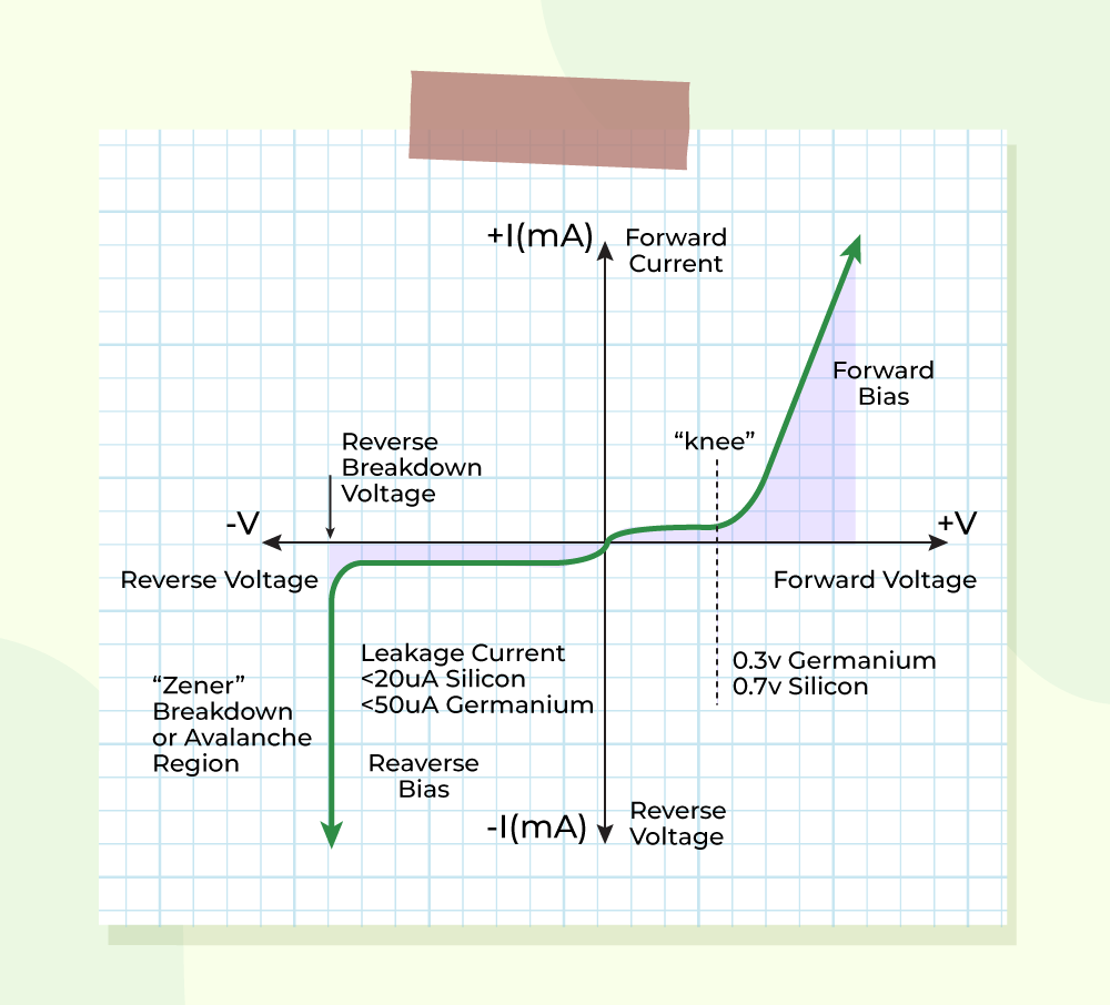
Figure 1 shows the I-V characteristic for a silicon P-N junction. Diffusion capacitance is also sometimes referred as storage capacitance.The Volt-Ampere or V-I characteristics of a p-n junction diode is basically the curve between voltage across the junction and the circuit current.This junction is known as PN junction.
Diode Resistance
Learn what a diode is, how it works, and how to make a p-n junction diode. Zero Bias – No external voltage potential is applied to the PN junction diode. Diodes can be used as rectifiers, signal limiters, voltage regulators, switches, signal modulators, signal mixers, signal demodulators, and oscillators.Diode law current–voltage curves at 25 °C, 50 °C, .Most commercially available PN Diode Switching Times have reverse recovery time t rr in the range of a few nanoseconds to 1 μs.Pn junction diode, terminals and its importance is discussed in detail. Created by Mahesh Shenoy.In this video, the PN junction diode has been explained. This makes the n region lose free .
Manquant :
explainThe p-n Junction (The Diode)
Learn how a pn junction diode is formed by doping p type and n type semiconductor and how it works under unbiased, forward and reverse biasing conditions.A pn junction is a combination of a p-type semiconductor material and an n-type.
(Part 1
One diode is used in a half-wave rectifier while two or four are used in a full-wave rectifier. And the working of this PN junction diode under forward and reverse bias has been explained.
Manquant :
explainPN Junction Diode and Characteristics of PN Junction Diode
It is a two-terminal or two electrode semiconductor device.A PN junction diode is a two-terminal electronic device that is made up of a PN junction.
![Complete Guide to PN Junction Diode [Updated] - Characteristics](https://www.tutoroot.com/blog/wp-content/uploads/2022/08/frame_0_delay-0.01s.jpg)
Why We Use Them.Diffusion capacitance occurs in a forward biased p-n junction diode. In this “semiconductor basics” series, we’ll learn about the properties of the .
PN Junction Diode and V-I Characteristics Explained
For example when I added this diode into a simple LED circuit mounted to a breadboard, I get a voltage drop reading of 0. A PN junction is formed . The electrical circuit can be made 'on' and 'off' by.The p–n junction in any direct band gap material emits light when electric current flows through it. For germanium diodes, when the voltage is 0. Units are available, however, with a t rr of only a few hundred picoseconds. This happens due to the concentration gradient across p and n sides.In this video, What is PN junction diode and How it Works in forward and reverse bias has been explained. The diode can conduct if a positive voltage (for the p-type) is applied and a negative voltage (for the n-type).
Manquant :
explain PN Diode Switching Times : A P-N junction diode may be used as an electrical switch.electricalbaba. (b) Reverse battery bias attracts carriers toward battery terminals, away from the junction. The circuit connection for determining the V-I characteristics of a pn junction is shown in the figure below. It is denoted as C D.Qualitative Effect of Bias. Explore the effects of . Specifically, current will flow readily in one direction (forward biased) but not in the other (reverse biased), . The second terminal is taken from the N .Learn how a PN junction is formed when an N-type and a P-type semiconductor material are fused together, and how a depletion layer and a built-in potential difference are created.The P-N Rectifying Junction.Manquant :
explain It is the simplest form of semiconductor device and is used as a rectifier, .; In circuit diagrams, a diode represents a triangle with a line across one vertex.Energy Diagrams of PN Junction & Depletion Region
Reverse Bias – The voltage potential is connected negative, (-ve) to the P-type material and . A diode has two terminals; one terminal is taken from the P-type layer and it is known as Anode.What are the characteristics of the P-N junction diode?A PN junction diode permits the current flow in one direction only. Understand the P-N junction theory, forward . Applying a potential to the ends of a diode does NOT increase current through drift. Find out the symbol, appearance, and types of diodes and how they are used in circuits.The PN junction. A p-n junction diode allows current when it is forward-biased and blocks the current when it is reverse-biased.What is PN Junction Diode:When both P-type and N-Typ.
![Complete Guide to PN Junction Diode [Updated] - Characteristics](https://www.tutoroot.com/blog/wp-content/uploads/2022/08/VIcharacteristics.png)
This junction is known as PN .Properties of pn – junctionThe p–type semiconductor has holes and the n–type semiconductor has free electrons as the . in which A is the cross-sectional area of the junction, and F i is the number of incoming photons per unit area, per unit time, with energy over the band-gap energy, and F o (V) is outgoing photons, given by = (). There are two operating regions and three possible “biasing” conditions for the standard Junction Diode and these are: 1. It does not obey Ohm’s law and Kirchhoff’s law of current electricity. What is an Open-Circuited P-N Junction? June 14, 2021 by Lorenzo Mari. A semiconductor diode is a P-N junction diode.PN junction is formed in a single crystal by joining two N-type and P-type semiconductors.The recombination at the junction allows battery current to flow through the PN junction diode. This creates a region of depletion where electrons and holes can be separated. The reverse current effect damages the junction. Here, we will take a look at the pn junction diode, terminals and how it's used. A p-n junction diode can be forward or . Hence, diffusion capacitance is considered in forward biased diode. Questions Tips & Thanks. What if we put them together? In this video, let's explore the famous PN junction.How does the PN junction diode form?A PN junction diode is formed by joining a P-type and an N-type semiconductor where the P-type region contains more holes and the N-type region con. It is a semiconductor diode that only conducts in one way, namely forward.

These are the characteristics of the PN junction diode or the characteristic curve of pn junction diode.