Flip flop logic gate
Fig: The logic symbol for the master slave S-R flip- flop does not use a dynamic-input indicator, because the flip-flop is not truly edge triggered. The RS Flip Flop is considered as one of the most basic sequential logic circuits. Flip-Flop Types, Conversion and Applications. As NAND gates contain current amplification, they can also be used to provide a suitable clock signal or timing pulse with the aid of a single . It has two inputs S and R and two outputs Q and . In this tutorial, we will discuss about one of the basic circuits in Digital Electronics knows as the SR Flip Flop. When Clk is low (0) Q retains its value/state regardless of what the Data . Akshay Singhal.View all products.A flip-flop is the basic memory element for storing a bit of information. Flip Flop in digital logic is a memory element capable to .Standard cell-based ASIC: This type of ASIC uses predesigned logic cells called standard cells, such as gates, multiplexers, and flip-flops. This lab continues our exploration of transistor switching circuits to include CMOS logic gates, latches, and flip-flops.SR flip flop, also known as SR latch is the basic and simplest type of flip flop.
SR Flip Flop Design with NOR Gate and NAND Gate
This master-slave implementation triggers .
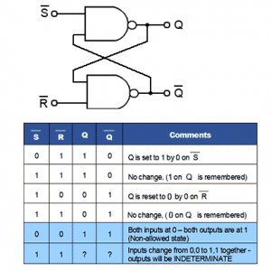
Given below is the logic diagram of an SR Flip Flop. The Flip Flop gate works by toggling its output signal whenever its receives a low-to-high logic transition on its input. (gates are the fundamental element for combinational circuits) Flip-flops are essentially 1-bit .Flip Flops Types- There are 4 types of flip flops- SR Flip Flop, JK Flip Flop, D Flip Flop, T Flip Flop.Gates and flip-flops are used to perform these functions in what is called a logic circuit. The basic block diagram . This SR Latch or Flip flop can be designed either by two cross . An SR flip-flop is the simplest type of flip-flop. Consequently, and edge-triggered S-R circuit is more properly known as . SR NOR latch truth table. The basic NAND gate RS flip flop circuit is used to store the data and thus provides feedback from both of its outputs again back to its inputs. The J-K flip-flop outputs reflect the J and K inputs upon the pulse of the clock, but remain locked until then except in the case where J=K=1 where the outputs simply flip upon a pulse.A flip flop is a sequential logic circuit that has some form of built-in memory. From the above circuit, it is clear we need to interconnect four NAND gates in a specific fashion to obtain an SR flip flop. It is a single bit storage element.Bistable – A flip-flop that has TWO stable states producing a single pulse either HIGH or LOW in value. Publisher Name.Aiysha Nazeerkhan | Published March 22, 2020 | Updated April 9, 2020.11 is as follows: When value of EN is low, both AND gates are disabled (i. Learn how CMOS SR latch and flip-flop devices work.It is obvious from the logic diagram that Q output has been connected or feedback with bottom NAND gate whereas Q output connected with top NAND gate (that’s JK flip-flop is a double feedback circuit).
Manquant :
flip flop The circuit consists of several logic gates that result in two stable states (a logic level 0 or 1), making a flip flop a bistable . These devices are available in a variety of input/output configurations and multiple package options to meet a wide range of design requirements. If the enable input is in the low (false) state, it will output a high impedance (hi-Z) signal. whatever the value of D, this value is not at all . A flip-flop circuit can stay in a binary state continually (as long as power is transferred to the circuit) before conducted by an input signal to switch states. Figure-1:R-S flip flop circuit diagram.An XNOR gate will perform a boolean XNOR function on its input signals.The JK Flip FlopThe D-type Flip FlopFlip-flop types, their Conversion and Applications
Whenever we enable a multivibrator circuit on the transitional edge of a square-wave enable signal, we call it a flip-flop instead of a latch. The J-K flip-flop is constructed using NAND and NOT gates as shown. It is more like a latch that follows its input during the entire interval that C is 1 but changes its output to reflect the final . Below shown a RS flip-flop constructed using a NAND gate same we can construct a RS flip flop using a NOR gate.
JK Flip Flop and the Master-Slave JK Flip Flop Tutorial
It is an edge-triggered device.
Lecture 9: Flip-flops
Flip flops are an application of logic gates.
From Logic Gates to Registers: Exploring the 74HC173
A D Flip Flop can be constructed from two D Latches and a NOT gate as . SR Latch using NOR gate. The Flip Flop is a one-bit memory bi-stable device. A simple flip-flop has two stable states (remember, for instance, that a capacitor has two states: charged and discharged). Publisher Logo. A Tri-State propagates the signal it receives, if it's enable input is high (true). It has only two logic gates . In this article, we will learn to. These flip-flops .1) RS flip flop. logic symbol (b) simplified truth table . Therefore, value of data input D has no impact on output Q whatsoever (i. It is commonly used as a basic building block in digital electronics to .
Manquant :
According to the table, based on the inputs the output changes its state. Search for both synchronous and asynchronous Boolean memory storage options in our vast portfolio of more than 900 counter, flip-flop, latch and register logic functions.Logic Gates are the building blocks of digital circuits that perform various logical operations on binary signals.Temps de Lecture Estimé: 6 minD-type Flip Flop Counter or Delay Flip-flop
outputs can be set to store either 0 or 1 depending on the inputs.Gates and Flip-Flops. You could achieve this without the pulse detector circuit by replacing the D Latch with a D flip flop (which is edge triggered). GATE Study Material. Flip-flops are the fundamental element of sequential circuits. In initial state output can in any state SET or RESET.
RS Flip Flop
You can also find related articles on how to convert, compare, and implement different logic gates. The SET-RESET flip-flop includes two NOR gates and also two NAND gates. Describe the D-flip flop using the three levels of abstraction . This circuit is a positive edged-triggered circuit owing to a double inversion via NAND gates. Spread the love.
Edge-triggered Latches: Flip-Flops
Its outputs only depend on the .
The D Flip-Flop (Quickstart Tutorial)
Flip-Flops
The ladder logic RS and SR flip flop in a PLC have SET and RESET inputs that are used to toggle the state of the flip flop output. The Q and Q’ represents the output states of the flip-flop.The Toggle Flip-flop is another type of bistable sequential logic circuit based around the previous clocked JK flip-flop circuit.Dive into the world of Logic Circuits for free! From simple gates to complex sequential circuits, plot timing diagrams, automatic circuit generation, explore standard ICs, and . Now from the above diagram it is clear that, this allows the J input to have effect only when the circuit . We will explore simple shift-register .
Flip-Flops & Latches
November 22, 2021 by Lorenzo Mari.Sequential Logic – The NAND Gate SR Flip-Flop. It doesn’t do anything when it receives a high-to-low logic transition. they stop operating). In other words, inputs are enabled (or operate) only on the . Ngõ vào điều khiển không đồng bộ: Khi ngõ khiển này ở mức tích cực (active) thì Flip-flop hoạt động theo cách nào đó. SR NAND latch truth table. One way of producing a very simple clock signal (or pulse) is by the interconnection of digital logic gates. The D-type flip-flop operates in a very simply manner: When Clk is high (1) the output, Q, is set to the value of Data (0 or 1) at that moment in time. The operational process of D flip-flop shown in the figure 5. Working of RS flip-flop depends on its inputs.12 – D flip-flop (a).The NOR Gate RS Flip Flop. It has two inputs, one is called “SET” which will set the device (output = 1) and is labelled S and another is known as “RESET” which will reset the device (output = 0 .A D-Type Flip-Flop circuit is built using four NAND logic gates connected as follows: We represent a D-Type Flip-Flop Circuit as follows. Gate level Modeling of SR flip flop. Learn the definition, types, uses, and examples of logic gates with GeeksforGeeks, a computer science portal for geeks. When you toggle a light switch, you are changing from one state (on or off) to the other state (off or on).The D Flip-Flop is an edge-triggered circuit that combines a pair of D latches to store one bit. So, the first time it . The state of the flip flop output will only revert back to FALSE if the RESET . In SET , S=1 and R=0.Ngõ vào dữ liệu D (Data): Trị logic hay trạng thái chính cần chốt.
Logic gate
That is, it reacts to the edge of a pulse. Below shown a RS flip-flop constructed using a NAND gate same we can . First, start with the module . When the SET input is TRUE, the state of the flip flop output is maintained TRUE, even if the SET input changes state back to FALSE. The old two-input AND gates of the S-R flip-flop have been replaced with 3-input AND gates .
The “clocked J-K . The D-type Flip-flop overcomes one of the main disadvantages of the . The output of each gate is . Standard cells are made using full .
![D Flip Flop [Explained] in detail](https://eeeproject.com/wp-content/uploads/2017/09/D-flip-flop-logic-circuit.jpg?is-pending-load=1)
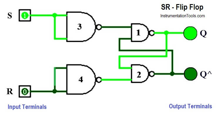
The simplest way to make any basic single bit set-reset SR flip-flop is to connect together a pair of cross-coupled 2-input NAND gates as shown, to form a Set-Reset .Flip Flop Gate. You can change the input values D and E by clicking on the corresponding buttons below to see the impact on the outputs Q and Q. They effectively store a single binary digit of state. S-R flip-flop represents SET-RESET flip-flops. There are a variety of flip-flops available that differ on how that state is manipulated. SR Flip Flop Construction using 4 NAND Gates: Basic Block Diagram of SR Flip Flop. Toggle flip-flops can be used as a basic digital . Form what I understand you are trying to build a circuit (using on logic gates) that toggles an LED on the rising edge of the input. SR flip flop logic circuit.
ASIC Design Flow: What is ASIC Design?
Multivibrators with Monostable, Astable and Bistable
A flip-flop is a .Flip-flops are the basic piece of sequential logic.Technical Article. This is equivalent to what happens when you provide a logic-high input to a T flip-flop: if the output is currently logic high, it changes to logic low; if it’s currently logic . The flip-flops are basically the circuits that maintain a certain state . (gates are the fundamental element for combinational circuits) Flip-flops are essentially 1-bit storage devices.An SR Flip Flop (also referred to as an SR Latch) is the most simple type of flip flop.SR Flip Fop using two NOR and two AND Gates. In the logic, called transistor-transistor logic (TTL) signals of a standard size (0V and +5V) . You can change the input values D and E by clicking on the .Flip Flop Types.And the third input of each gate receives feedback from the Q and Q’ outputs.What is a digital latch? What are the types of latches? SR Latch using NAND gate.The circuit diagram of the J-K Flip-flop is shown in fig.
4-bit counter using D-Type flip-flop circuits
Most simple arrangements of logic gates can be described by a truth table that defines all its output values as a logical function of its current input values.
Tổng quan về Flip-Flop và ứng dụng
The JK flip flop is basically a gated SR flip-flop with the addition of a clock input circuitry that prevents the illegal or invalid output condition that can occur when both inputs S and R are equal to logic level “1”.
Sequential Logic Circuits and the SR Flip-flop
The state of this latch is determined by the condition of Q.