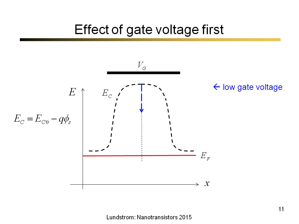
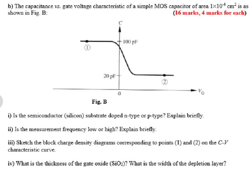
Peak gate voltage

Abstract: In this article, a double closed-loop self-regulating active gate driver (DCSAGD) for power device is proposed.7 Maximum required DC gate current to trigger IGT TJ = - 40 °C Anode supply = 6 V resistive load 270 mA TJ = 25 °C 150 TJ = 125 °C 80 TJ = 25 °C, for 40TPS. The IGBT switches slower; see also table 1.
Understanding Peak Source and Sink Current Parameters
A case study that compares different drivers and peak currents. That mean, when DIAC trigger, voltage across DIAC is > 30V Since diac . 1: Peak Detector Schematic to detect peak voltage over the external gate resistor [11] Nevertheless, its traditional use and repeated evidence of correlation with mean junction .5 A Reverse Peak Gate Voltage (Pulse Width ≤ 1. For temperatures of about 25 o C, SCR gate trigger voltage is typically 0. The voltage change -dvCE/dt and the current change diC/dt during the turn-on process may be influenced by varying the gate resistor RGon. The external gate resistance is assumed to have a negligible temperature .Influence of peak gate current and rate of rise of gate current on switching behaviour of SiC MOSFET Abstract: Emergence of SiC technology brought revolutionary reforms in power . The closed-loop control strategy is realized at low cost by all .Application Note
Application Note AN-983
10b) show that peak current decreases rapidly as the temperature is increased from 1. VGT GATE TRIGGER VOLTAGE The gate .2倍即可。 V: VGD: Non-triggering gate voltage: 门极不 . Note that all curves are typical, with no minimum or maximum limits, and derived at 25 °C.Maximum peak negative gate voltage - VGM 10 V Maximum required DC ga te voltage to trigger VGT TJ = - 40 °C Anode supply = 6 V resistive load 4. Experimental results for a 1200-V silicon carbide MOSFET gate driver are presented, demonstrating the switching loss of 230 μJ at 800 V and 10 A.
The measurement method involves detecting the peak voltage over the external gate resistor of an insulated-gate bipolar transistor or mosfet during turn-on.09KW to 1200KW.3 V VGD VD = VDRM RL = 3.The source peak current equation in this simplified model is I PK_SRC = V DD / (R DS (ON)_P + R EXT ), and the sink peak current is I PK_SNK = V DD / (R DS (ON)_N + R .45 V threshold voltage.
可控硅参数说明及中英文对照表
It is important to note at what test condition this peak current is specified.
Power MOSFET Basics: Understanding the Turn-On Process
Park Gate & Company
When the membrane potential passes -55 mV again, the activation gate closes.
Gate Voltage
2005Afficher plus de résultats It specifies the maximum instantaneous value of forward blocking voltage across the SCR excluding all .orgRecommandé pour vous en fonction de ce qui est populaire • Avis
TRIAC Peak gate voltage
The measurement method involves detecting the peak voltage over the external gate resistor of an insulated-gate bipolar transistor or MOSFET during turn-on.3 msec, TA = 25°C) PG(AV) 0.2 V IH IT = 500 mA Gate open MAX.Timed with the peak of depolarization, the inactivation gate closes. Since VDS is fixed. The impact of such voltage stress can .peak voltage over the external gate resistor . These peak values are evaluated by comparing the mathematical results with simulation results by PSIM and the errors .PNP increases with current and an increase in gate voltage causes an increase in channel current, that is the base drive of the PNP, hence a reduction in voltage drop across the PNP.0 V *Operating Junction Temperature Range TJ −40 to +110 °C *Storage Temperature Range Tstg −40 to +150 °C Stresses exceeding Maximum Ratings may damage the device. Thus, a gate driver that is . 50 mA IL IG = 1. xx ------------ (3) dt gs.V GT: The minimum positive gate voltage required to turn on the SCR. The voltage-gated K + channel has only one gate, .Download scientific diagram | (A) the threshold voltage (Vth), (B) peak transconductance (gm,peak), and drain current density at the gate overdrive voltage of 2 V (Id@Vg − Vth = 2 V) as the . In this system, the Fermi levels or work-functions could be changed under the back-gate bias. This means that at the off-state, the SCR has to withstand at least (√2) per peak line voltage. AU - Anthony, Philip H.A method to reduce switching losses is proposed, using a resonant gate driver to absorb parasitic inductance in the gate path, enabling the gate resistor to be removed. 2012Cutoff, Triode and Saturation6 janv.

This represents a 20% reduction in switching . The voltage VGS is the actual voltage at the gate of the device, and it is .If the peak gate current and voltage swing of the gate driver are known, these values can be used to calculate a value for R Gint.

Triangular wave generator in FPGA14 mars 2019[PIC] AC Power Control with Thyristor: Phase Angle Control using triac with PIC.The source peak current equation in this simplified model is IPK_SRC = VDD/ (RDS (ON)_P + REXT), and the sink peak current is IPK_SNK = VDD/ (RDS (ON)_N + .0 s, TA = 25°C) VRGM 8.The LM5109A is the high-voltage gate drivers designed to drive both the high-side and low-side N-channel MOSFETs in a half-bridge configuration, full-bridge configuration, or in a synchronous buck circuit.0 TJ = 25 °C 2. The threshold voltage, commonly abbreviated as V th or V GS(th), of a field .

Peak Working Forward-blocking Voltage V DWM. At lower temperatures the gate voltage required to keep the device in the . a) find the value of Rag series resistor in gate circuit to limit the peak power dissipation in the gate 5 watts. N2 - Parasitic inductance in the gate path of a Silicon Carbide MOSFET places an upper limit upon the switching speeds achievable from these .3 kΩ Tj = 125 °C MIN.comParasitic Inductance and Capacitance-Assisted Active .
Thyristor theory and design considerations
An electrical method for junction temperature measurement of MOS-gated power semiconductor devices is presented.For higher gate voltages, when the MOSFET has been fully turned on, any operating point will be located in the area shaded in green to the left, marked as the resistive (or ohmic) region.Park Gate has been supplying new and re-conditioned electric motors since 1946 and during this time we have built up a reputation for providing an excellent standard of reliability and service. For single phase voltages, the power grid with the highest RMS level is 277 V.

This allows for N-channel MOSFETs control in half .SCR is used in series with the load and the line voltage in most applications. 90 mA dV/dt VD = 67% VDRM Gate open Tj = . This is a crucial parameter in .The multi-stacked heterolayers were characterized through the KPFM setup with applied V BG to examine the surface potential variances of each 2D layer depending on the back-gated voltages, as presented in Fig.VRGM Maximum peak reverse gate voltage 5 V j = 25 °C, unless otherwise specified) Symbol Test conditions Value Unit IGT VD = 12 V RL = 33 Ω MIN. V GT varies with the operating temperature, load resistance, forward blocking voltage, and gate-cathode resistance.
Parameter list for SCRs, Triacs, AC Switches, and Diacs
Increasing the gate resistor reduces the voltage and current changes.When the voltage at the gate crosses the threshold voltage of the MOSFET, the drain-to-source volt-age begins to fall (the MOSFET begins to become en-hanced). The capacitive parasitic turn-on may be obviated by reducing .
Conductance Peak
The gate voltage is maintained at the desired level using a feedback loop.Lastly, the voltage measured across the 0.
The influence of gate voltage on voltage drop and peak current capability is very much dependent on the spe-cific device design.Calculation of SCR Power Loss, Gate Resistor Example 1: An SCR has a V g – I g characteristics as V g = 1.
A detailed explanation of this method is provided in [11]; however the basic measurement principle will be outlined in the following paragraphs.Abstract: In power conversion systems, the power devices often need to block high voltage levels during the OFF-state.The peak gate oscillation voltage can also be evaluated in two different cases. The peak current can therefore be approximated by Ohm s Law, I § V/R.orgMOSFET Gate Driver Circuit Design for High Repetitive . Some gate drivers yield higher typical drive current at higher bias voltage.0 sec, TA = 25°C) PGM 0.Forward Peak Gate Power (Pulse Width ≤ 1.How is peak current defined? For a Triac, a bias condition between the gate and main terminal MT1.comGate Drivers and Gate Driving with SiC MOSFETs | . Note that any spurious voltage/current spikes at the gate must be less than Vg (min) and Ig(min) to avoid false triggering of the thyristor.Temperature-dependent I – Vg measurements of the conductance peaks (Fig. Maximum Ratings are stress ratings only.: peak gate current This is the maximum peak current allowed through gate and cathode, defined for 20 µs pulse duration.The gate voltage is maintained at the desired level using a feedback loop. This represents a 20% reduction in switching losses in comparison to that of conventional gate drive methods. After that, the inactivation gate re-opens, making the channel ready to start the whole process over again.T1 - High-Speed Resonant Gate Driver with Controlled Peak Gate Voltage for Silicon Carbide MOSFETs.Peak reverse gate voltage This parameter is only defined for SCRs.5 V TJ = 125 °C 1.0 V Operating Junction Temperature Range @ Rated .
AN2006-01
SCR Specifications and Ratings
1-Ωsense resistor will give the engineer a value calculated from measurement of the peak drive current using Figure 4 and Ohm's law. Experimental results for a 1200 V Silicon Carbide MOSFET gate driver are presented, demonstrating switching loss of 230 μJ at 800 V, 10 A.Very Low Forward “On” Voltage at High Current.Analysis of false turn-on phenomenon of GaN HEMT with parasitic inductances for propose novel design method focusing on peak gate voltage Abstract: GaN HEMT is generally . For higher temperatures of about 100 to 125 o C , V GT drops to approximately 0.Here you see diac connected to GATE of TRIAC and DIAC trigger voltage ~30V.0 sec; TA = 25°C) VRGM 5.It turns-on thyristor successfully. 2013Ac Voltage regulator using Triac17 avr.Auteur : Texas Instruments, Incorporated [SLLA387,A]
Basics and Design Guidelines for Gate Drive Circuits
RG: peak reverse gate . AU - McNeill, J N.1 W Forward Average Gate Power (t = 8. Low−Cost TO−226 (TO−92) Pb−Free Packages are Available* MAXIMUM RATINGS (TJ = 25°C unless otherwise noted) . This has been found to be . This voltage is directly proportional to the peak gate current, .The measurement of the internal gate resistance can be based on a superimposed high-frequency measurement signal on the gate voltage in either on-or offstate [11], [13], [34], [35], via DC gate .New Resonant Gate Driver Circuit for High-Frequency . Functional operation above the Recommended Operating . Experimental results for a 1200-V silicon carbide MOSFET gate driver are presented . in a certain application, the gate voltage consists of rectangular pulses of 12 V and of duration 50μs with duty cycle 0.02 W Forward Peak Gate Current (Pulse Width ≤ 20 s, TA = 25°C) IFGM 0.*Reverse Peak Gate Voltage (Pulse Width 1.