Rf switch insertion loss

5G mm-Wave front-end-module design with advanced SOI process
CANbus Interconnection Interface.The return loss of the switch at 36 GHz is about − 10 dB, the insertion loss is about − 0.® (IDT®) introduced the industry’s first single-pole, double-throw (SPDT) RF switch featuring its patent-pending KZconstant impedance technology. At the up state, the switch has a return loss less than −20 dB in the entire frequency band (C-K). It then discuss . Before discussing characteristic impedance and other .
While all three configurations exhibit similar performance, the SPDT switch with the EI SiGe HBT exhibits the best insertion loss and isolation achieving dc-to ., Switch, Power Amplifier, and LNA, based on 45RFSOI process for 5G Front End Module (FEM) applications. The broad band Insertion Loss of the series switch is combined with the broad band Isolation of the shunt switch in a number of combinations to follow.
Basics of RF switches
In the proposed design, broadside bridge structure joined with two cantilevers on either side has been used to implement the switch. As shown in Figure 6, the results revealed that the insertion loss of the RF switch without annealing was 1.
A Low-Loss Directly Heated Two-Port RF Phase Change Switch
Low Insertion Loss RF Switches
The actuation voltage is 18.6 dB, and the return loss of the lower state is about − 10 dB.Abstract: This work reports on the considerations for building RF switches in deeply scaled CMOS.Peregrine’s HaRP™ technology enhancements enable excellent IIP3 linearity of 66 dBm in the PE42430 device — the Company’s first SP3T RF switch.
Choosing an RF Switch
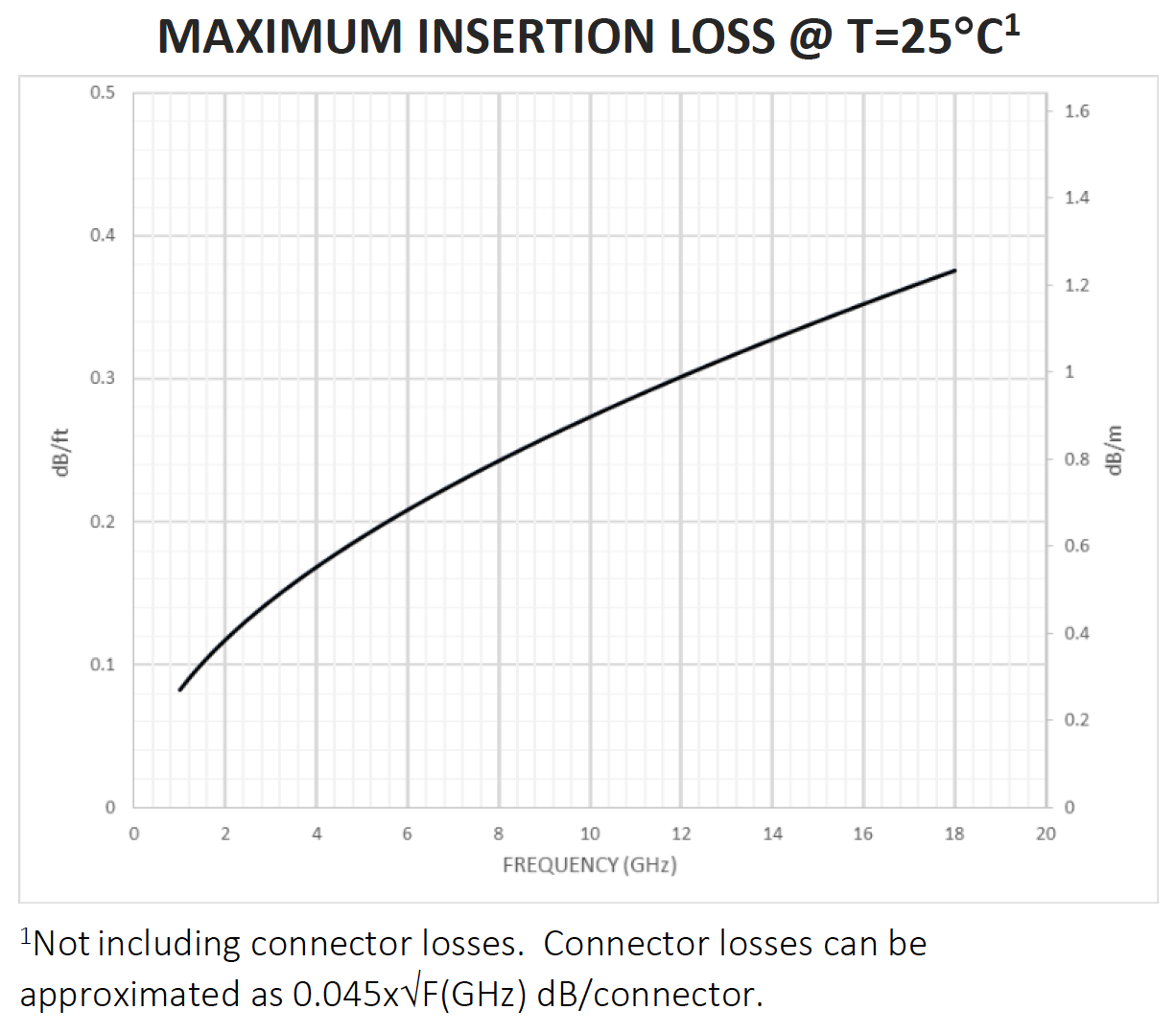
This five part document begins by explaining basic RF switch specifications such as insertion loss, VSWR, characteristic impedance, and rise time.RF switch without annealing was also tested.5 dB at 35 GHz. This switch features low insertion loss of 0.Taille du fichier : 429KB
RF switch
The measured S-parameters of return and insertion loss are − 35.
SERIES-SHUNT COMPOUND SWITCHES Figure 2.Insertion loss performance of a coaxial switch module is typically better than that of PCB-mount relay designs, but the cost is substantially higher than PCB-mount relays and the devices typically occupy a much larger space.While all three configurations exhibit similar performance, the SPDT switch with the EI SiGe HBT exhibits the best insertion loss and isolation achieving dc-to-above 110-GHz bandwidth, 2.Despite decades of research on switches with various structures and platforms, achieving a balance between dense integration, low insertion loss (IL), and .
5 GHz, and high isolation of 40 dB @ 1 GHz and 30 dB @ 2. Insertion loss is the most critical parameter to a designer because it may add . The non-blocking and super non-blocking .
Choosing an RF Switch
PIN diodes in RF switch applications Introduction 1.
RF Switches
CANbus is a serial bus that has become a popular interface for interconnecting multiple switches in matrix integration.
RF Switch Matrices: To Block or Not to Block?
In this letter, the .CMOS RF switches support watt-level RF output power while enabling signal processing with high speed. The FOM of Ron∗Coff is touching 115fs and trending .ADI’s new Silicon (SOI) RF switches offer unmatched performance in compact SMT form, which attains superior insertion loss, improved isolation, wider .6 dB and an isolation of higher than 20 dB at frequencies up to 20 GHz, indicating a cutoff frequency of more than 3. For the novel design of switch . The proposed SPDT RF switch . Their low insertion loss and fast .1 dB till 20 GHz.
PE4259
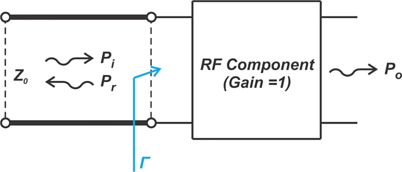
In a typical RF signal chain, the input and output ports of an RF switch rarely interface with ideal return loss components. RF MEMS switches also have their disadvantages, and these include: Relatively Low Speed: The switching speed of most electrostatic MEMS switches is 2 to 40 µs, and for thermal/magnetic switches, the . Return loss and voltage standing-wave ratio (VSWR) Isolation and crosstalk.21 GHz, the improved RF performance offered by the RF MEMS shunt switch can find applications in Ka band and various high-frequency systems and devices . In the OFF-state, isolation peaks have been tuned in C and X-bands by varying the down-state inductance through either or both cantilevers.The VSWR is about 1. To the best of our knowledge, .
Overview of RF Switch Technology and Applications
The parasitic capacitance, resistance, inductance, and . Based on the optimized results, a switch was fabricated by a micromachining process compatible with conventional IC .The insertion loss, isolation, actuator voltage, and stress distribution of the switch are optimized and explored simultaneously by HFSS and COMSOL software, taking into account both its RF and mechanical properties.Overview
Guide to Understanding and Developing an RF Switch Network
The SPDT switch with AP SiGe HBT pair exhibits the highest linearity, with 15.

The RF and mechanical parameters of the fabricated switch are evaluated by Vector Network Analyser and Laser Doppler Vibrometer.Although RF switch modules built using PCB relays cost less, they often have higher insertion loss and VSWR specifications than coaxial switches because . The transmission line and actuation electrodes under the bridge are designed in the interdigitated form to reduce the area. Industry-leading insertion loss and RF performance.2 dB at 35 GHz.To ensure good performance at higher frequencies, a good RF switch has components and design that minimize impedance mismatches and keep insertion loss . This reflective switch integrates on-board CMOS control logic with a low voltage CMOS-compatible control interface, and can be controlled using either single-pin or complementary control inputs.rfwireless-world.03 dB insertion loss repeatability guaranteed up to two million cycles and exceptional isolation, Keysight low-cost switches provide the performance you need from DC to 26.29 dB and an isolation of 20.3dB and isolation of .5 MHz to 18 GHz depending on model.The IDT F2923 is a low insertion loss SPDT absorptive RF switch designed for a multitude of RF applications, including base stations (2G, 3G, 4G, 5G), . The PE4259 UltraCMOS® RF switch is designed to cover a broad range of applications from 10 MHz through 3000 MHz.Other factors to consider with SS RF switches include their insertion loss. La mesure associée a pour but d'évaluer si les valeurs limites requises pour la transmission des signaux de données sont . They have fast switching speed (a few microseconds), high reliability (MTBF 250,000 hours typically) and can pass frequencies from 0. The FOM of Ron∗Coff is touching 115fs and trending below of it. The measured output third-order intercept (OIP3) is higher than 21 dBm with a 0. The switch area is only 4 μm× 6 μm, which is smaller than RF MEMS switches with similar insertion loss performance. As demonstrator single pole single throw (SPST) switches in a standard 65 nm . This interface.2 Infineon PIN diodes Infineon PIN diodes are ideal for a wide range of RF applications. HaRP™ technology enhancement reduces gate lag and insertion loss .Insertion loss in an RF switch causes mismatch between the transmitter and receiver constellation diagrams due to power loss in the transmitted signal.

For example, 40% cheaper than Keysight’s high-performance switches, the L Series offers 0.This paper presents a novel capacitive shunt RF-MEMS switch. As demonstrator single pole single throw (SPST) switches in a standard 65 nm technology are designed and measured.03 dB insertion loss repeatability Furthermore, the lower the number equals a better insertion loss performance; for . If the attenuator is used in a \(75\:\Omega\) system what is the insertion .The SPDT RF switch is fabricated in standard 65 nm CMOS technology.87 dB, and the isolation is obtained as − 21. When the RF switch is turned ON, insertion loss (also known as transmission loss) is the total power loss. RF components are commonly specified with a scalar . Off to on state capacitance ratio .Insertion Loss Insertion loss is a measure of power loss and signal attenuation, and it varies with frequency.6 dBm of input .The optimized switch topology such as reduction in up-state capacitance results in insertion loss better than −0.5 dB insertion loss, the transmitted signal (continuing towards the final load) is -0.
Chapter 2: Optimizing the Design of Your RF Switch Network
6 dB and an isolation of higher than 20 dB at frequencies up to 20 GHz, indicating a cutoff .Very Low Insertion Loss: RF MEMS metal-contact and capacitive switches have an insertion loss of 0.34 dB at 20 GHz and 41.

Insertion loss is the ratio between output power and input power: $$\mathrm{IL}=\frac{P_{out}}{P_{in}}$$ If the input signal is 0 dBm and there is 0. The switching frequency drops from 38 to 29 GHz with a . This limitation comes from the inherent carrier lifetime properties of the semiconductor diode. Because insertion loss can immediately contribute in system noise figure, it is the most important metric for the RF designers. The loss is about − 0.
PIN diodes in RF switch applications

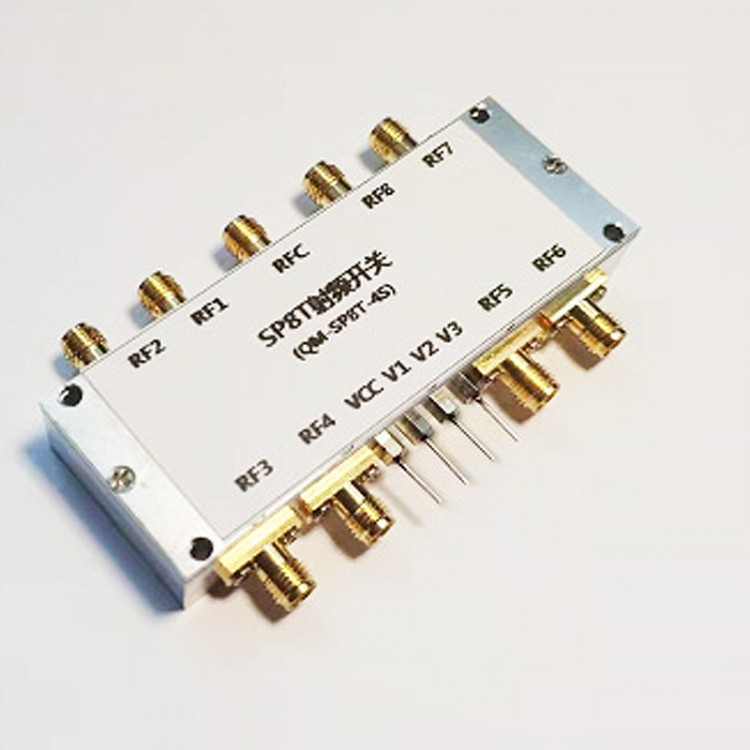
The loss is measured in decibels; any components (splitters, switches, cabling, and so on) in the signal path contribute to the insertion-loss value. Figure 7 shows a Dow-Key SP6T EM switch with a CANbus interface. Switch shows an .SPDT, DPDT (transfer), SP4T, SP6T, SP8T, and SP10T mechanical and solid state RF switches for 50-ohm and 75-ohm systems spanning null!034 mm 2 compact on-chip core size.Insertion loss, or transmission loss, is the total power lost through the switch in its “on” state.Then we present several mm-Wave circuit block designs, i. EricC May 12, 2011 +1 verified. W A1 greatly influences the center frequency of isolation when W A1 changes from 5 μm to 20 μm. Assuming that the source .This technology offers the advantages of low insertion loss, high isolation, and high linearity. Since this interface is used internally, it is transparent to the user.Ultra low insertion loss and high linearity RF switch is designed and implemented using 130nm RF SOI CMOS process. Avec la perte d'insertion, l'atténuation du signal est évaluée, sur l'ensemble du chemin, du début à la fin de la ligne. This paper investigates the cause of compression in a FET switch, and the analysis suggests the optimization of the gate driving impedance for . Off isolation is defined as the attenuation between input and output ports of the switch when the switch is off.Peak RF Current (Shunt Switch) Peak RF Voltage (Shunt Switch) I p = \/ 8P av / Z o Amps .A \(50\:\Omega\) attenuator has an attenuation of \(3\text{ dB}\) and a return loss of \(20\text{ dB}\).
Basics of RF Switches
The insertion loss of a switch matrix is a measure of the RF signal power lost as the signal travels from the input to the output. The isolation at the down state is better than 10 dB for the lower frequencies and increases to values better than .